
Miniaturization of IoT
More battery life and smaller IoT devices are resulting in optimized performance, and our team is excited to partner and lead.
In this digital era, as we wirelessly connect more and more devices to the Internet, researchers and engineers face several challenges, like how to package a radio transmitter into their existing device real estate, how to make increasingly smaller devices, how to reduce the area coverage for mounting chips. They are also striving to meet consumer demand for Internet of Things (IoT) products that are ergonomically easy to use.
Ideally, engineers would tend to use IoT components that are smaller in size, have better RF performance, and have reasonable prices. However, these characteristics do not usually converge in IoT component offerings, and that presents a challenge for solution providers.
Fortunately, the size of a silicon die has been getting smaller and smaller over the years as the industry adopts new silicon manufacturing processes. The industry has been solving the space issue for IoT implementations by combining the MCU and RF frontend into system-on-chip (SoC) configurations.
The demand for embedded SIM (eSIM) is steadily rising among the smartphone manufacturers, laptop manufacturers, energy & utility sector companies. The OEMs across the globe are focusing on the development and integration of eSIM in numerous applications.
The increasing demand for miniaturization of IoT components across various industries is also boosting the demand for eSIM globally.
In 2018, researchers from the Green IC group at the National University of Singapore (NUS) in collaboration with associate professor Paolo Crovetti from the Polytechnic University of Turin in Italy created the timer, that trigger sensor to perform their tasks when required, is believed to be so efficient that it runs using an on-chip solar cell with a diameter close to that of a human hair. This is a major step in IoT miniaturization claimed with low-power.
The wake-up timer can continue operations even when a battery is not available and with very little ambient power, as demonstrated by a miniaturized on-chip solar cell exposed to moonlight. An on-chip capacitor used for slow and infrequent wake-up also helps reduce the device’s silicon manufacturing cost thanks to its small surface area of 49 microns on both sides.
IoT sensor nodes are individual miniaturized systems containing one or more sensors, as well as circuits for data processing, wireless communication, and power management. To keep power consumption low, they are kept in sleep mode most of the time, and wake-up timers are used to trigger the sensors to carry out a task. As they are turned on most of the time, wake-up timers set the minimum power consumption of IoT sensor nodes. They also play a fundamental role in reducing the average power consumption of systems-on-chip.
When designing a hardware module, one of the pressing questions is about Antenna. Developers must work around the space reserved for antenna and the type of antenna they will use to integrate with a corresponding module. PCB trace antennas are general preference because of their low bill of material (BoM) costs. But they require a significant size which can cause devices to be large and difficult to work with.
The smaller size we try to achieve, the less efficiency we can have for the RF performance. Chip antennas are famous for various applications as they simplify design efforts and optimize size consumption.
According to statistics of Bluegiga, approximately only 10 percent of these evaluated designs deploy the external antenna, and 90 percent of the customers choose modules with a built-in chip antenna. Hence, it becomes necessary to continuously evaluate the possibility of space reduction on chipboard, something Cloud of Things has successfully achieved with our latest DeviceTone Genie product line, working with great partners including Nordic Semiconductor and AES with their minIot devices.
Stay tuned for more information on how Cloud of Things and our DeviceTone engineers are working with our partner ecosystem to continually advance smaller form factors with powerful capabilities.
Similar Blogs

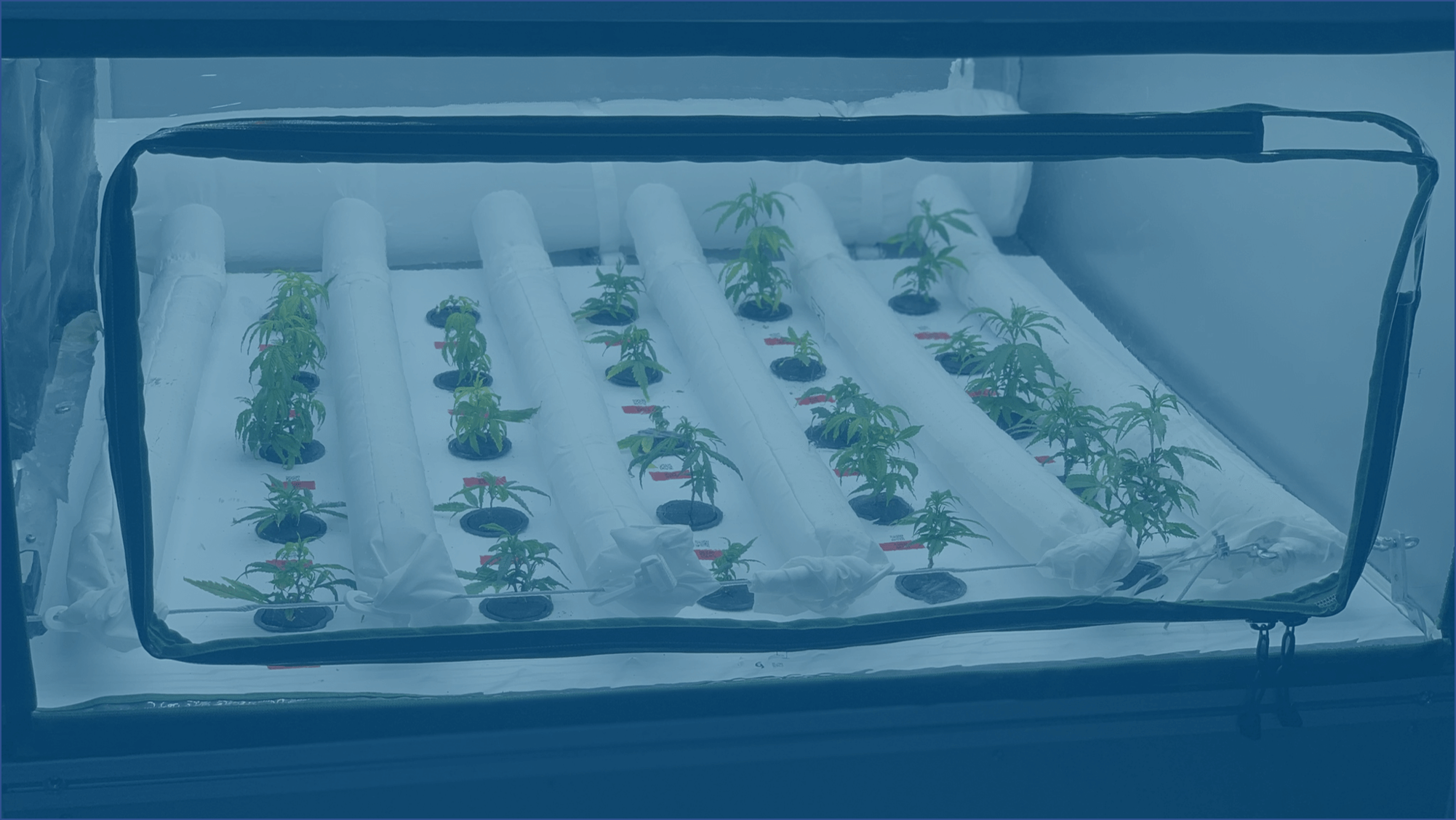
As global demand for high-quality medical cannabis skyrockets, Hortica, Cloud of Things, and AES announce innovative cultivation initiative
Hortica, a technology-oriented company that is developing and manufacturing an advanced platform for cultivating plant-made pharmaceuticals today announced it has selected Cloud of Things and AES to partner on a major innovation initiative that will accelerate the implementation of Hortica’s breakthrough which makes it possible for growers of cannabis and of other medicinal plants to supply organic, safe, consistent and standardized crops to patients, clinical trials and pharmaceutical industry.
Proud to Partner with Pioneers: Cloud of Things and AES Support the Launch of Hortica
Today , one of our customers, Hortica, announced their entry into the U.S. market followed by global expansion. Working with our partner AES (minIoT) we helped Hortica create an advanced “connected cultivation” solution supporting the growth of high quality, high yield crops.

Innovation in Israel With Global Impact: Proud to Be Part of the Israeli and Global Tech Communities
A couple of months ago, I had the privilege to join Cloud of Things as the new CEO, and while I had experience in running very large information technology operations and R&D groups for the IDF and for the Central Bank of Israel, where I was most recently CIO and a member of the board, I didn’t have direct experience in the massive and dynamic Internet of Things world.